Writing axle’s GameBoy emulator
Reading time: 31 minutes
Table of contents
✱ Note
The Nintendo GameBoy is an exceptionally well-documented system, perfect for anybody who’d like to take a crack at emulation. Publicly-maintained resources like the Pan Docs make it both approachable and convenient to get an overview of the GameBoy’s address space layout, to understand the mechanics of hardware peripherals, and to learn about various edge-case behaviors that some games depend on.
Over the past three weeks, I’ve been writing a GameBoy emulator my very own. This is not a unique project! I was inspired by the blog post of another adventurer doing the same thing. What’s the special sauce of this post, then? Rather than stopping at writing an emulator alone, I threw an extra requirement into the mix: The emulator should run and be playable under axle, my from-scratch and home-grown operating system. Before I dive into the nitty-gritty, it’s worth asking: is this even feasible in axle’s present state?
Ah! Well then, off we go.
axle doesn’t (yet!) have the debugging facilities and development niceties that make modern software development possible, let alone pleasant. Therefore, we’ll have to work with some kind of dual-approach: it should be easy to both run the emulator on my macOS machine, for quick iteration, and to run it under axle when we’re ready to test the whole shebang.
Most software I develop for axle gets the simple only-runnable-within-axle approach, in part because most software that runs within axle uses axle-specific platform APIs for things like window/event-loop management and message passing. However, I’ve chosen the multi-platform approach for more complicated bits of software: the first one where this dual-pronged approach paid off was axle’s first iteration of a browser.
axle desktop with browser visiting axleos.com, April 2021
Okay, let’s get started! I’m not totally new to emulation - I’ve written a fairly comprehensive AArch64 simulator - but one thing that’s new to me is emulating an entire system, complete with hardware peripherals, rather than just CPU and memory. Nevertheless, the beating heart (and great starting point!) of any emulator will be the CPU implementation. Let’s have a think about what our goals are here.
The CPU
All CPUs operate via the same fundamental cycle: fetch, decode, execute. Modern CPUs throw some spectacularly complicated wrenches into the mix, but for our purposes we’ll keep it simple.
Let’s break it down.
The fundamental data type of a computer is a fixed-size integer (these days, 64 bits). Again - we’re going to gloss over details like SIMD and hardware floating-point. If you know more, think of this as your moment to feel smug. Every song you’ve ever digitally consumed, PDF you’ve browsed, game you’ve played, or message you’ve sent boils down to streams of these numbers. This is not a particularly esoteric idea! What’s slightly more interesting, though, is that the code that’s facilitating these tasks is also just a stream of numbers.
Where is this code and data stored? In some kind of memory, typically RAM, that the CPU can access and operate on.
Let’s take a concrete example. Say our RAM contains some numbers like the following (expressed in hexadecimal):
48 65 6c 6c 6f 2c 20 77 6f 72 6c 64 21The meaning of these numbers is entirely contextual! It could be some kind of data, yes: a piece of encoded text, a few encoded pixels within an image, a list of salaries (let’s hope not!), etc. Or, it could also be code: raw instructions that the CPU knows how to interpret to perform an operation. The way the bytes are interpreted, and therefore the meaning that gets derived from them, depends on the context in which the bytes are used.
In the example above, those bytes are the result of me encoding some data - in particular, the string “Hello, world!” - character-by-character into numbers, using the ASCII character encoding. Let’s take another example:
48 8b 04 25 00 00 00Again, there’s no absolute meaning to these bytes, but the context in which I intend for them to be understood is as a piece of code to be run on an x86_64 CPU. An x86_64 CPU would understand that this sequence of bytes is telling it to move a number from one register to another. Another way of expressing the same thing as those bytes would be to write mov $rax, $rbp, but the details aren’t particularly important right now.
We could even have a sequence of bytes that can be understood as a perfectly valid sequence as either code or data:
6a 6bIf an x86_64 CPU tried to interpret this sequence of bytes as an instruction, it’d understand it a directive (or instruction) to “push 0x6b to the stack”. If we tried to interpret it as ASCII-encoded text, we’d instead understand this sequence as the text “jk”.
These mappings are entirely conventional! Why does 6a correspond to j when interpreted as ASCII text? There’s no ‘fundamental’ reason. Through accidents of history, one particular way of mapping bytes to English characters proliferated enough for everybody to agree to formalize the mapping into a ‘dictionary’ called ASCII✱. Similarly, how does an x86_64 CPU “know” that 6a should mean PUSH? Just the same, AMD and Intel defined what an x86_64 CPU should be able to understand. When an assembler is generating code for this platform, it knows to emit this byte when it wants the CPU to run a PUSH instruction. When CPUs are manufactured in their billion-dollar fabrication plants, circuitry is lasered into the silicon that ensures that when the CPU reads the 6a byte from memory, the CPU will do the corresponding operations associated with what we’d expect PUSH to do.
✱ Note
Okay, where were we going with this? Yes! CPU’s like to fetch, decode, and execute. The fundamental loop of a CPU is:
-
Fetch the next byte from memory.
-
Decode the byte, interpreting it as an instruction the CPU knows how to understand.
-
Execute the instruction, updating the system with the result of the operation indicated by the instruction.
How does the CPU know where to fetch from? All CPUs contain an instruction pointer ✱ denoting where it’s currently fetching a byte from. This pointer would otherwise move along in a linear fashion, but one of the central tricks of computers is that this pointer can also be redirected, jumping backwards and forwards as the logic of the code dictates. This enables some neat use cases, such as winning WWII.
✱ Note
Back to the GameBoy. It’s got a CPU, so we know it’ll be running a fetch, decode, execute loop. But what is it fetching its code from? The game cartridge slotted into the device! This cartridge will hold all the code and data necessary to run the game.
Hold on a second. We know that the Fetch stage gets the next byte from memory. What about the very first byte? How is the CPU going to start running code located in the game cartridge at all?
The boot process
Earlier, I mentioned that code and data is stored in memory, typically RAM. Not always. There are special cases that vary based on the system - whether it be a GameBoy, a UEFI-based computer, an iPhone, etc.
When a device first boots, systems need some way to set themselves up enough to move on to something more advanced: this next step might be loading an operating system, handing off control to a game cartridge, or something else. This piece of code is purpose-built for the boot process, and it’s also typically etched into the silicon of the system when it’s manufactured. In other words, it’s read only memory, or ROM. Thus, this piece of code is generally referred to as the boot ROM.✱
✱ Note
Hrm. We’ve established that the boot ROM is the first thing that runs, but really we’ve just pushed our question further back a bit. How does the CPU begin running the boot ROM when the system first starts up?
When the CPU is initialized, the aforementioned instruction pointer will contain the value 0. That is, the CPU will kick off its fetch-decode-execute lifecycle using whatever bytes are at the very beginning of memory.
So, our system needs some way to arrange things such that when the CPU reads byte# 00, it gets the first byte contained within the boot ROM, and so on for byte# 01, byte# 02, etc.
Enter the MMU. One way to think about memory is as a big list of bytes. Reading byte# 00 is equivalent to reading the first element of the list, while reading byte# 100 is equivalent to reading the 10016th✱ element of the list. Pretty straightforward. These byte indexes are alternatively called ‘addresses’, and the list itself is alternatively called a ‘space’✱. Thus, we get the term address space.
✱ Note
✱ Note
✱ Note
The CPU can read (or write, sometimes!) to each of these addresses, but where is the “other end”? Where is the data at these addresses stored? A first guess might be RAM, which is certainly on the right track. That said, it’s not the whole story.
The MMU, or memory management unit, mediates the CPU’s access to different hardware peripherals that are connected to the address bus, of which RAM is just one. When the CPU tries to access a given address, it’s the MMU’s job to determine which piece of underlying hardware that particular address belongs to, and to forward the access to that device as appropriate. The MMU even handles when the CPU tries to access a piece of memory that no device is providing. Different systems implement different behavior when something like this happens - some will generate an internal event that invalid memory was accessed (x86_64 does this), some will have the MMU return all zeroes or all ones when an invalid address is read (the GameBoy does something like this).
With that knowledge in hand, it gets a lot easier to answer our question about how the boot ROM is executed: the MMU on the GameBoy has things set up such that when the CPU reads address 0, it will receive the first of the boot ROM’s bytes that were etched into the silicon when the GameBoy was manufactured.
Okay! Long walk for a short drink of water, but this knowledge will serve us well. Let’s track the sequence of events so far:
-
The GameBoy receives power
-
The CPU sets its instruction pointer to 0
-
The CPU fetches the byte at the address indicated by its instruction pointer
-
The MMU routes the read of address 0 to the boot ROM
-
The first byte of the boot ROM is returned to the CPU
-
(We are here!) The CPU decodes the byte into an instruction
Great! Our understanding has leveled-up from Fetch to the next stage, Decode.
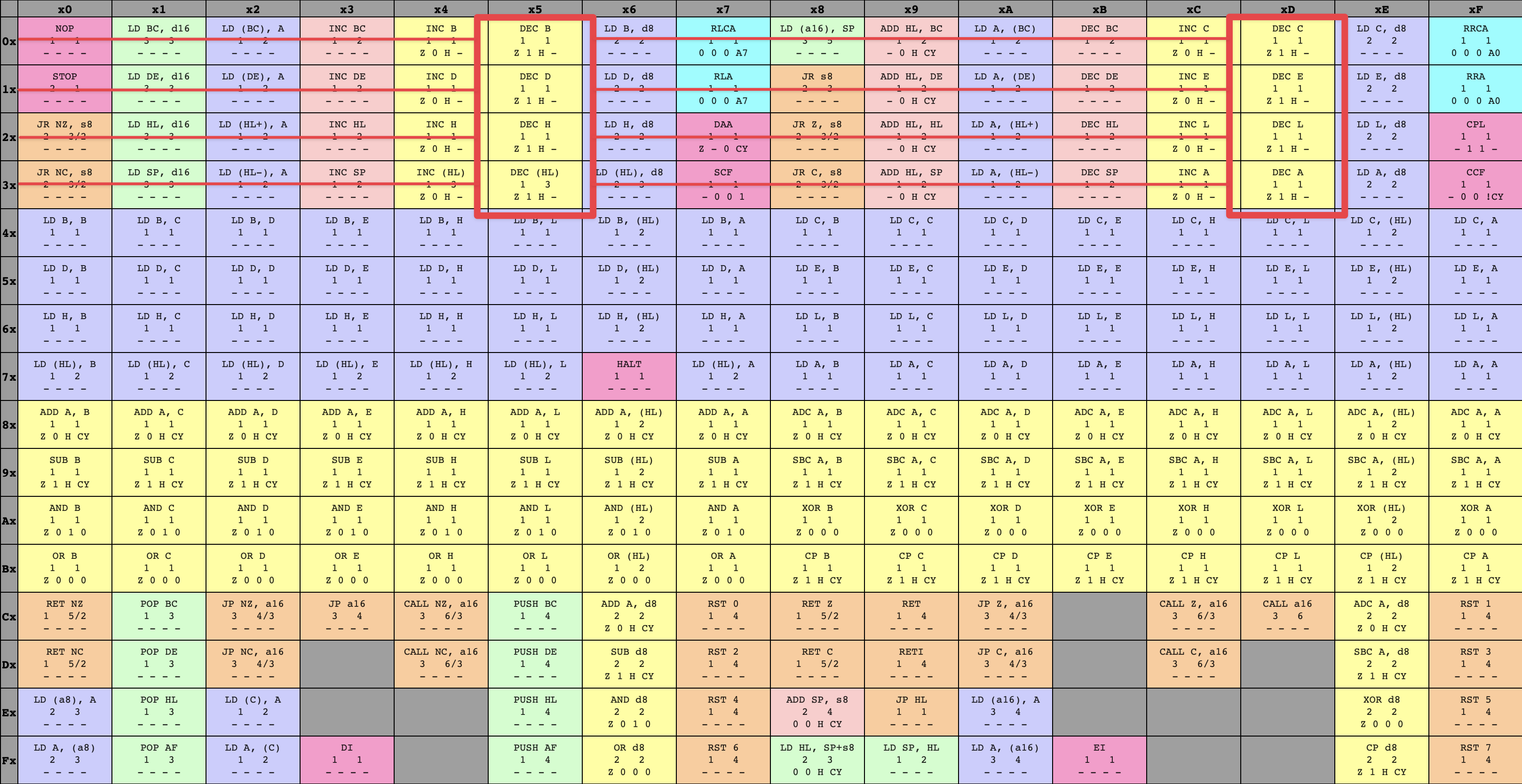
Instruction decoding
Like we discussed, the correspondence of a number to its meaning when decoded as a directive to the CPU is contextual and dependent on the CPU in question. That said, there is a necessary level of shared understanding: the CPU itself and code that’s intended to run on that kind of CPU must agree on what each byte should mean. If we tried to run bytes compiled for x86_64 on a CPU manufactured to run AArch64, things would get very weird very quick because the semantic meaning of our code has been lost. This correspondence of numeric bytes to the directives or operations they’re associated with is termed the set of instructions that the CPU knows how to run, or the CPU’s instruction set.
The GameBoy’s instruction set is derived from that of the Zilog Z80. The lineage isn’t as important as the inheritance: like the Z80 it’s derived from, the GameBoy CPU runs an 8-bit instruction set. That is, instead of the fundamental data-type being the 64-bit integer we touched on above, the fundamental type is instead an 8-bit integer.
Each instruction starts off with an opcode, a 8-bit✱ value (or code) denoting what operation the CPU should perform.
✱ Note
For example, say the CPU fetches this opcode:
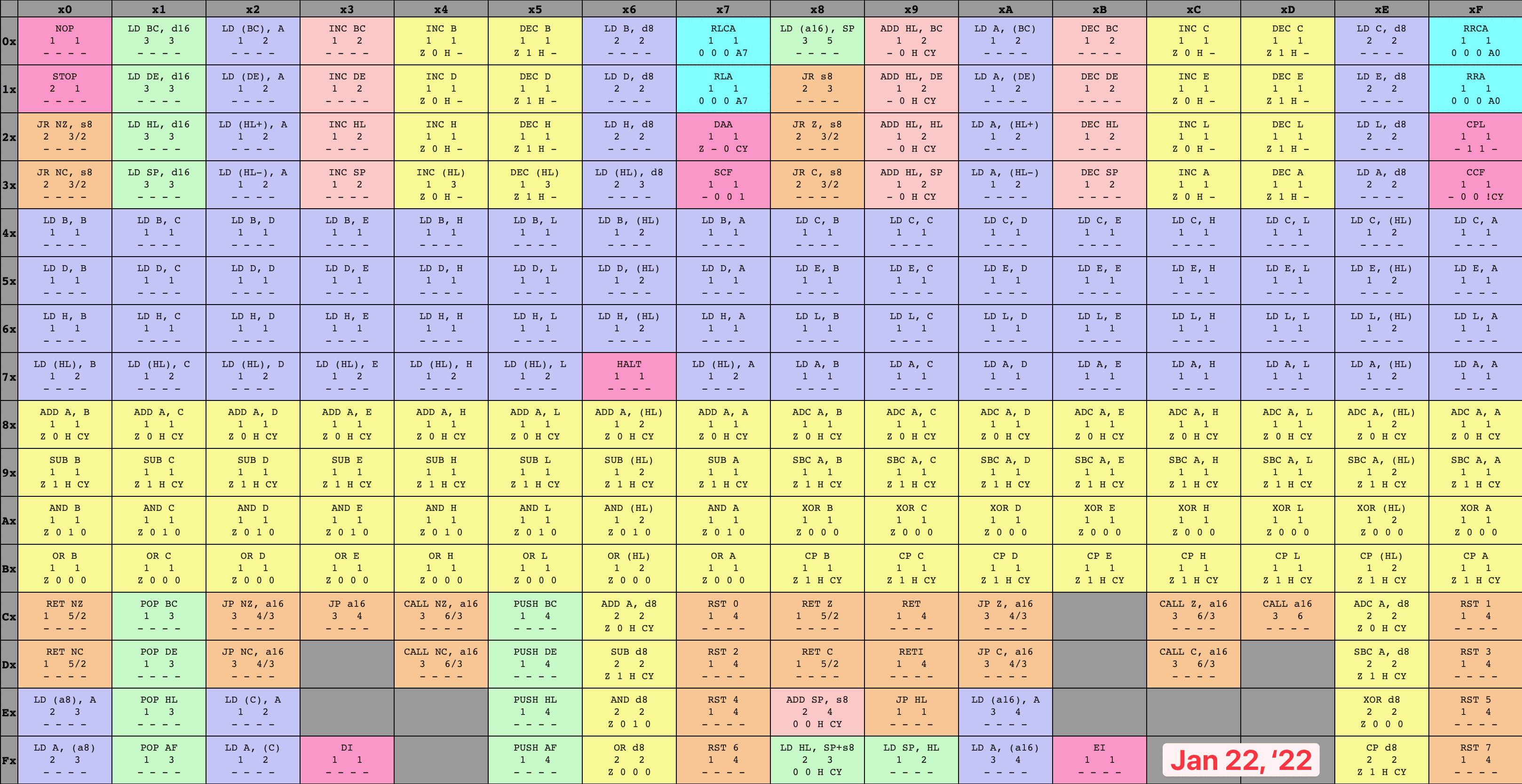
76What’s the contextual meaning for the GameBoy CPU of this opcode? The answer to this question is technically defined by the circuitry etched into every GameBoy CPU, but people have also come up with great visualizations of the GameBoy CPU’s instruction set to aid emulator writers. Here’s an opcode table from a great resource I used while writing my emulator:
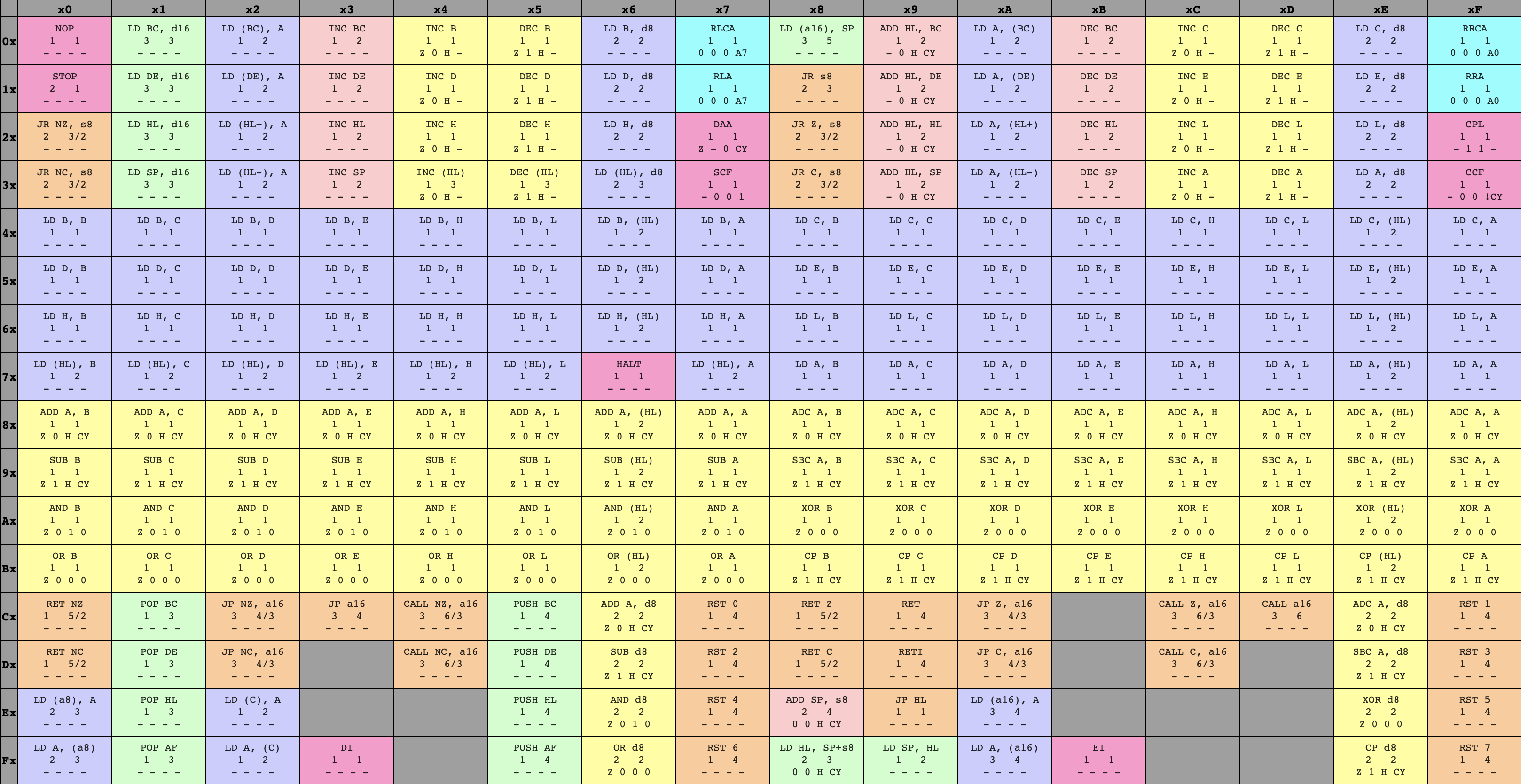
8-bit GameBoy CPU opcodes
By following the ‘7’ row on the left and the ‘6’ column across the top, we can see that the opcode 76 corresponds to an instruction called HALT. When the CPU fetches this opcode, it will decode the byte and understand that it refers to the HALT instruction, then will run the operation associated with HALT (we’ll get there, don’t worry!)
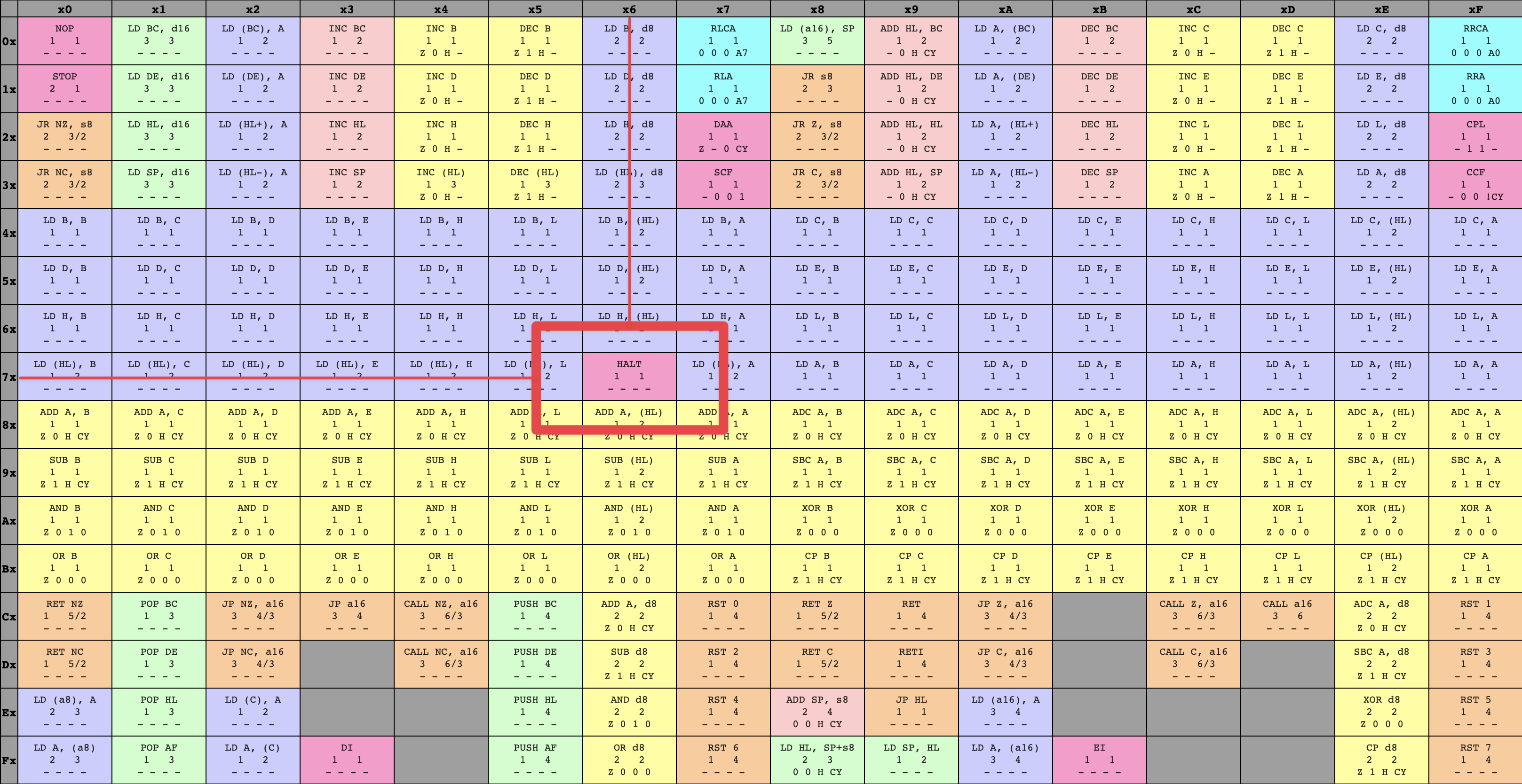
HALT instruction within opcode table
Some instructions can’t make do with just a single byte, but need some extra data to describe more details of their operation. For example, say the GameBoy CPU contained an ADD Register A, u8 instruction✱. The operation associated with this instruction would be to take the 8-bit value (the u8), and add it to the 8-bit value stored in Register A, then to store the result of the addition in Register A. Clearly, this is going to take more than a byte to store, because we need to know what 8-bit value to add to Register A. The 8-bit value will be stored directly following the opcode itself. Therefore, some instructions take up more than just one byte: we’ve got one byte for the opcode, plus either no data, 1 byte of data, or 2 bytes of data.
✱ Note
c6.This technically makes the GameBoy CPU’s instruction set a variable-length encoding, where the number of bytes it takes to store each instruction is dependent on what the instruction does. Some more contemporary instruction sets (particularly x86_64, another descendent of the 8080 lineage that the Z80 itself is descended from) get a lot more wacky with this, but thankfully the GameBoy CPU caps the maximum instruction size at three bytes.
Armed with the knowledge that an instruction can span multiple bytes, let’s take a look at the full GameBoy CPU opcode tables:
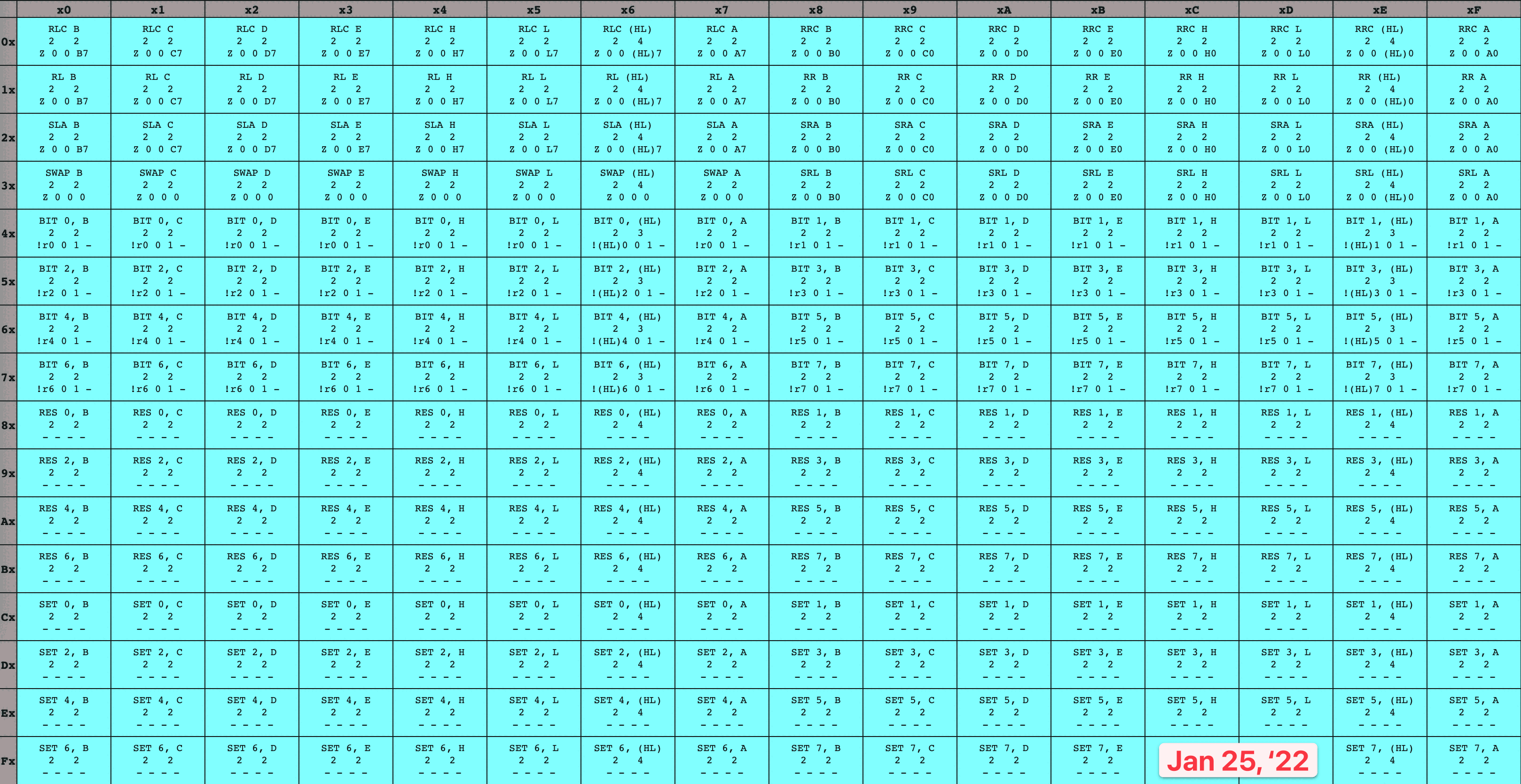
8-bit GameBoy CPU opcodes 16-bit GameBoy CPU opcodes
Whoa, did you catch that? Tables! Plural!
This is interesting, and shows where our digression about multi-byte instructions comes from: if every instruction took up exactly one byte, then there would be a maximum limit of 256 instructions in the instruction set, since a byte (equivalent to 8 bits) is capable of storing any number from 010 (000000002) to 25510 (111111112)✱. Thanks to the encoding scheme, it’s possible for the instruction set to define more than this. The GameBoy CPU ended up defining exactly 500 instructions✱.
✱ Note
✱ Note
d3 and ec. These opcodes are undefined by the instruction set, and the CPU will gingerly walk past them if ever faced with their unknown horror✱.✱ Note
While some of these instructions are multi-byte because they contain an extra byte of data (like our ADD Register A, u8 example), some of them are multi-byte because they contain an extra byte of code. Specifically, every instruction in the blue table has an initial opcode byte of cb, followed by a second opcode byte whose meaning is given by the table. I’ve seen this set referred to as the cb opcodes ✱.
✱ Note
cb opcodes provide many different bitwise operations on registers.So! We’ve got our opcode, plus perhaps an extra byte or two that it needs to do its work. It’s time to execute the instruction, updating the system state by performing the operation indicated by the opcode.
There’s an important point here: we have multiple opcodes because each opcode does something different to the system. Each unique opcode maps to a unique operation that the CPU knows how to perform, and our fledgling CPU emulator will need to know how to apply every one of them to our emulated system.
Getting clever with our implementation
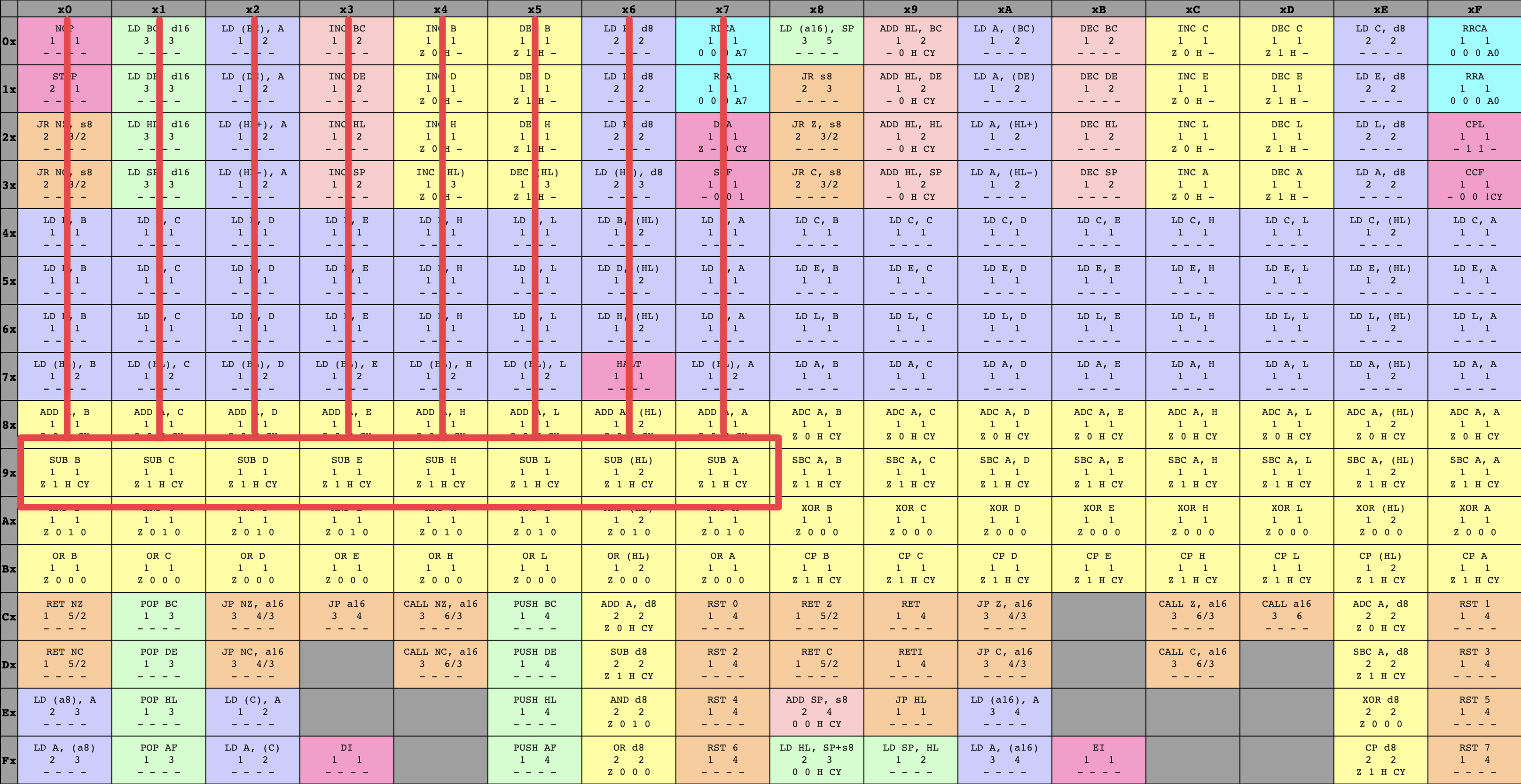
Thankfully, the task isn’t really so daunting as “implement 500 unique operations”. Many of the opcodes are variations on a theme. For example, let’s take a closer look at a snippet of the instruction tables from above:

SUB instructions
Each of these instructions starts off with SUB, then has a different letter it operates with. Looking at these opcodes as a whole, these are the possible letters that a SUB instruction may contain:
B, C, D, E, H, L, (HL), AEach of these ’letters’, of course, mean something very specific in the context of the system: the GameBoy CPU, like any CPU, computes with the help of registers. While 8-bit integers are the fundamental data type of the CPU, the register is the fundamental data storage of the CPU. Almost any time a CPU operates on an 8-bit number, it’s doing so by interacting with the contents of a register. When we want the CPU to read an 8-bit number, we use an instruction to load the byte located at a memory address into a given register. When we want to perform arithmetic, we specify the registers containing the numbers we want to operate on.
The GameBoy CPU has exactly eight registers. The names are arbitrary, but the GameBoy itself and our CPU table sheets call them:
B, C, D, E, H, L, A, FPerfect! These exactly match up with what we saw in the variants of the SUB instruction, so each SUB instruction is clearly a slightly different version that performs a subtraction using the register on the right hand side.
…
Oh.
Let’s see ’em side-by-side.
SUB operands:
B, C, D, E, H, L, (HL), A
CPU registers:
B, C, D, E, H, L, A, F
Well, that’s a complication. The possible SUB operands are very similar, but not identical, to the available CPU registers. And what is that (HL) doing there, anyway? Clearly, we’ve got some talking to do.
While what I said before is true, that the CPU mostly performs computations via loading data into registers, it’s not the full story. The CPU is also able to perform computations by talking directly to memory, without needing to involve an extra load/store with a register.
The GameBoy CPU provides exactly one way to do such a thing. With some instructions, the GameBoy CPU knows how to take the values in the H and L 8-registers, stick them side-by-side to create a 16-bit number, then read the value at the address indicated by the 16-bit number from memory. This operation of “reading the value at an address” is indicated by the () surrounding the HL, and is more generally referred to as dereferencing the address. We’ll see more of it later. But first! An example of what this would look like in practice✱:
✱ Note
H and L together into a 16-bit value, we place the value of H into the most significant byte, and the value of L in the least significant byte. This kind of multi-byte ordering is described by a system’s endianness.H: aa
L: bb
(HL): The byte currently stored at address aabbOkay, sure, along with the 8-bit registers we can also perform some operands by dereferencing the value in HL, or (HL) for short. Is that all?
Back to our SUB operands and available CPU registers, there’s another glaring omission: we can see that the CPU contains an F register, but there’s no SUB variant that supports it. What gives?
Well, the F register is special: rather than being a general-purpose 8-bit register like the rest, it instead serves as the special-purpose flags register. That is, over the course of execution of an instruction, the system might want to note some resulting state for further processing. For example, if the result of the SUB instruction is exactly zero, the Z bit in the flags register will be set. The CPU then has other instructions that do different things based on whether a particular flag is set or not. The F register isn’t directly accessible to the programmer; its various bits can be set as side-effects of running instructions, and its status can be implicitly read by running instructions that do different things based on its contents.
Right. We’ve got our SUB operands. When we fetch the opcode indicated by the instruction pointer, how will we know which SUB instruction to execute?
SUB instructions with opcodes
Of course, one way to do this is in a slightly brain-dead “if the opcode is 90 do this, if the opcode is 91 do that, …”, but I think we can do a bit better. Let’s write out all the SUB opcodes and see if we can spot anything:
90 91 92 93 94 95 96 97There’s a nice and simple property staring us in the face - it’s also quite visible from looking directly at the opcode table above. The SUB instructions start at 90, and increment by 1 for each right-side operand. Let’s take a look at the binary representation of each opcode:
90: 10010000
91: 10010001
92: 10010010
93: 10010011
94: 10010100
95: 10010101
96: 10010110
97: 10010111
We can see that each SUB opcode starts with the same pattern in the most significant bit: 10010___, followed by a sequence that counts up by 1 for each variant: 000, 001, 010, 011, 100, 101, 110, 111. This is convenient for us! It means we can do some pattern matching on whatever opcode byte we’ve fetched. If the high bits match the 10010 pattern that all SUB instructions follow, we know that we’ve fetched a SUB instruction, and all that’s needed is to take those lower 3 bits as an index into the table that will tell us which register to subtract with.
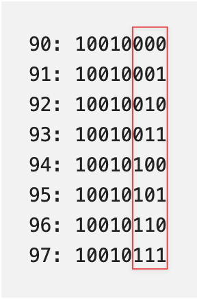
Incrementing index in SUB opcode encoding
Er. Not always a register - our friend (HL) is still around, ready to fetch memory at a moment’s notice.
This is really nice! With one fell swoop, we’ve managed to knock out eight instructions with one implementation.
One minor point I’ve glossed over up to know: We’ve got a SUB instruction, we’ve decided what register it’s subtracting with, but what is it going to subtract from? And where does the result of the subtraction go once we’ve performed it?
We’ve got another register with privileged status to discuss: the A, or accumulator register. A common concept among instruction sets, the A register is both an implicit operand to, and implicit destination of, SUB instructions (and many other instructions!) In other words, while the SUB instruction only mentions one operand on the tin, it actually performs an operation something like the following:
A = A - OperandAgain, this isn’t the whole picture: executing this instruction may also update various status bits in the F register, such as whether the result was exactly zero, whether the subtraction underflowed, and a few other conditions.
Let’s look at another instruction!
DEC instructions
The DEC instructions subtracts 1 from the operand and places the result back into the operand’s storage. In other words, it performs this operation:
Operand = Operand - 1This is straightforward in the case where the operand is a register, and requires just a hair more thought when the operand in question is (HL). Sketching out what that might look like, we get:
H = 11
L = 22
HL = 1122
In this case, we’ll be running DEC with the dereferenced value of HL, or the byte stored at address 1122. Let’s pretend this address already contains some value:
(1122) = 77When we run the DEC (HL) instruction, we’ll read the current value of (HL): first, we conjoin the 8-bit values of H and L, 11 and 22, to yield a 16-bit address, 1122. Then, we’ll ask the MMU to read the byte at address 1122, and we’ll get 77 back. Finally, we’ll subtract 1 from that value, and store the result back into the byte stored at address 1122. Nothing too snazzy here, but we’ll want to keep it in mind when designing our routines that can execute an instruction given any of its operand variants. Early on, I had to rework my first implementation so that it could reuse the same code to handle both plain registers and (HL).
The DEC family sounds straightforward enough. Can we do the same trick we pulled with SUB, in which we implement a bunch of similar instruction variants with a single implementation?
With SUB, things were pretty simple: the operand we were supposed to work with was clear, with a one-to-one correspondence starting from opcode 90. With DEC, things are looking a bit shakier: the various opcodes are on entirely different sides of the table, and certainly aren’t incrementing by one from one variant to the next.
Can we spot anything if we write out the DEC variants’ hexadecimal representations?
05
0d
15
1d
25
2d
35
3d
Hmm… There’s certainly a pattern here, but it’s not clear to me how we’d take a look at an opcode and immediately see both that it’s a DEC, and which variant it is. Maybe looking at the binary representations of each opcode will shed some light?
00000101
00001101
00010101
00011101
00100101
00101101
00110101
00111101
Yes! We’ve got the same pattern of three bits counting up one-by-one to describe what variant the opcode refers to, except this time around those three bits are sandwiched in the middle of the opcode! We can identify a DEC by checking whether the opcode matches 00___101, and those three bits in the middle tell us what operand we’ll be working with in the same counting-by-one fashion as before. I find this really interesting, because this pattern isn’t apparent at all when looking at how the opcodes are visually laid out in the table, but it’s really clear when writing out the binary representations of the opcodes!
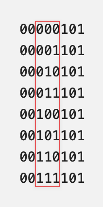
Incrementing index in DEC opcode encoding
That should be a pretty good foundation to get us going writing our emulated CPU in software. The thing about a CPU, though, especially when writing a virtual one, is that it gets a lot more useful when you’ve got some code you’d like to execute on it!
Running a program
We’ve got hundreds of opcodes to implement, and some kind of plan to divide-and-conquer will be vital to implementing this thing in an approachable way. If we pick an existing program that we’d like to run on our fledgling CPU, it’ll provide us with a great system for knocking out segments of the instruction set:
-
Load the program into our virtual environment
-
Kick off the CPU on its fetch/decode/execute lifecycle
-
Keep going until the CPU fetches an opcode it doesn’t yet support
-
Implement the missing opcode (and its relatives, if any)
-
Repeat!
But what program to pick? Ideally we’d want something that’s approachable in size (so we don’t have to implement every opcode under the sun before we see results), that’s well-understood (so we can check whether our emulated CPU is doing the right thing), and that’d be useful code to run anyway.
A great candidate here might be the boot ROM that executes every time the GameBoy boots! Let’s see:
-
Approachable in size? Yep, the boot ROM fits in just 256 bytes.
-
Well-understood? Undoubtedly - people have annotated the boot ROM’s instructions line-by-line.
-
Useful in its own right? The boot ROM is responsible for showing the classic
Nintendologo on startup, so I’d go as far to say this is essential.
That last point is a real classic, and very familiar to anyone who’s played a GameBoy: the scrolling logo is the start to every session! This means that the boot ROM both a functional program, and an iconic part of the GameBoy experience.
Now, it’s useful to understand what the boot ROM is doing exactly, so we know the shape of things to expect. We know that in general the boot ROM’s responsibility is things like initializing the rest of the system in such a way that later code can run in a known state, but the boot ROM can have other responsibilities, too. One of these responsibilities, both in the case of the GameBoy and many other systems, is verifying the integrity of the rest of the code the system will execute.
Trusting trust
This leads to a concept called the chain of trust. The boot ROM, as we know, is read-only, so if we trust the boot ROM and the boot ROM trusts whatever it loads next, we’ve established a chain ensuring that any code that the system runs is ‘safe’. The definition of ‘safe’ varies: it might mean that the code has been signed with a cryptographic signature, for example, assuring that the program has been verified and authorized by the platform vendor, or it might validate that the code hasn’t been tampered with after compilation.
The GameBoy, however, does no such cryptographic validation of the next piece of code to run after the boot ROM. Released in 1989, I am not sure whether this is down to cryptographic validation being too taxing for the constrained hardware that the GameBoy packs, whether the contemporary techniques for code signing had not been developed to a sufficient degree to enable Nintendo to cryptographically secure the games of third party developers, whether they simply weren’t able to pack enough code into the boot ROM to do cryptographic validation while balancing other tradeoffs, or some other reason. Nevertheless, the case remains that the boot ROM performs no such thing. That said, Nintendo still wanted some measure of control over the system! With any entertainment platform, there is a palpable propensity for end-user control and modification. The consequences of this can range from the outright cool (hobbyist games and demoscenes), to the explicitly negative for Nintendo and games publishers (pirated games redistributed without paying the developers).
Without any way to technologically enforce that all software running on the GameBoy must be authorized by Nintendo, is there some other way to enforce this?
Yes indeed! Nintendo did something very clever here. Remember the classic Nintendo logo that scrolls down from the top of the screen when the boot ROM executes? Rather than including the Nintendo logo data in the boot ROM and loading it into the video RAM data directly, Nintendo required that every game cartridge contained its own copy of the Nintendo logo.
Do you see the trick here?
…
It’s a threat.
Nintendo is staving off pirates and unauthorized redistributions by threatening them with copyright law. To ship an unauthorized or pirated game, the pirate is forced to distribute the Nintendo logo too. Clever!
One interesting consequence of this is that every GameBoy cartridge ever manufactured contains the same redundant copy of the Nintendo logo, over and over again in duplicated silicon counted in millions, all to threaten would-be pirates.
Except… how does the boot ROM know that the logo stored in the cartridge is the correct logo at all? Couldn’t we just put anything in there and allow the boot ROM to display it?
Well, yes!
We can stick anything we’d like in the cartridge memory that’s supposed to contain the Nintendo logo. Here’s what the boot screen looks like if we don’t initialize the cartridge logo memory at all✱:
✱ Note
ff for uninitialized reads, this is also what you would see if you booted the GameBoy without a cartridge inserted.Invalid Nintendo boot logo
Seems like a pretty simple circumvention for Nintendo’s litigative DRM, no? Unfortunately, when I called the cartridge logo redundant, I really meant it: the boot ROM contains its own copy of the Nintendo logo, too. It doesn’t display it, though: it reads the logo data from the cartridge, displays it, then checks it against the copy of the logo stored in the boot ROM itself. If there’s any kind of mismatch, the boot ROM will lock up the system to prevent any further use.
Going back to the task at hand: we want to run the boot ROM code as a tool to help move us along our CPU implementation, but to run the program we’ll first need to have the program in the first place. How do we know what code the boot ROM contains?
Acquiring the boot ROM
This might seem straightforward at first glance: the boot ROM program has been etched into the silicon of every GameBoy ever produced, so can’t we just… read it?
Well, yes, in theory we can. Practically, though, reading data from a physical medium measured in micrometers is no small feat. In fact, it took 14 years before someone managed to do it, armed with no less than a powerful microscope, a GameBoy CPU with the plastic housing chemically dissolved away, and a whole lot of gumption.
Thanks to their work, copies of the boot ROM, both in ready-to-run compiled bytes and annotated assembly, are floating ‘round on the net - waiting for any intrepid emulator developer who’s ready to take them on.
Hrm. Hang on a second. 14 years to read the boot ROM? Couldn’t a game just, like, read out the contents of the boot ROM addresses when the game starts running, then display the data on the screen or something?
Well, yes. That’s why Nintendo included one more trick in the jam-packed 256 bytes of code in the boot ROM. Recall our earlier digression on the MMU:
When the CPU accesses an address, the MMU will route the access to the peripheral that ‘owns’ that address. Say the CPU reads address #00. This is within the boot ROM, so the first byte of the boot ROM will be accessed. What about address #ff? Still within the boot ROM, so the MMU will route the access there. And address #100? The boot ROM takes exactly 256 bytes to store, so this is just outside the boot ROM’s address space. Instead, the MMU will route this access to a different peripheral: the game cartridge.
With our idea above, the game cartridge would read addresses #00 through #ff, storing or displaying their contents so that a human could read the boot ROM data. Why doesn’t this work?
As its final flourish, the last 4 bytes in the 256-byte boot ROM encode the following 2 instructions:
Address: #00fc    Byte(s): 3e 01    Description: Load Register A with 01
Address: #00fe    Byte(s): e0 50    Description: Load (ff50) with Register A
Feeling enlightened? Me neither. Let’s head to the Pan Docs to see what’s so special about the address #ff50.
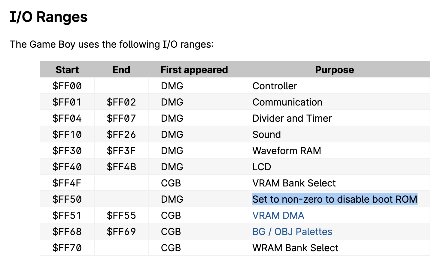
Memory-mapped IO descriptions
Ah ha! Similarly to how the MMU will redirect any accesses to the boot ROM address range to the boot ROM itself, the MMU also implements some special addresses: accessing them (via reads or writes, depending) triggers special system behavior. Writing a value of 1 to address #ff50, in particular, causes the MMU to effectively disable the boot ROM! After this value has been written, the MMU won’t forward any accesses in the address range #00 - #ff to the boot ROM any longer. Instead, the MMU will direct these accesses to the game cartridge. There’s also no way to disable this behavior once enabled, short of rebooting the system!
In other words, the very last thing the boot ROM does, just at the cusp of the instruction pointer iterating past the #00 - #ff range, is write a special value that’ll cause the MMU to disable any and all ability to reach the boot ROM data via memory access. This is spectacularly well-timed, as the moment the CPU is finished running this instruction, its instruction pointer reaches #100 and it leaves the #00 - #ff range it was previously running within. The game that’s been loaded has no way to talk to the boot ROM, but there is the bonus that the game is free to use the #00 - #ff range for its own purposes✱.
✱ Note
OK, acid and microscopes it is. Let’s recap the major functions of the boot ROM program:
-
Initialize the system
-
Load the Nintendo logo from the game cartridge
-
Scroll the logo onto the screen
-
Validate the logo’s validity
-
Disable the boot ROM and allow the cartridge to begin running its code
The nice thing about writing an emulator is we don’t need to know exactly how the emulated program does each of these things! All we really need to do is provide the environment that the program expects itself to be running within, and to run its code faithfully. The program will do the rest. This is a really powerful idea: it means that we can write an emulator that runs popular games, without us ever needing to know how those games work under the hood. In fact, our emulator is theoretically equivalent to any computer. That is, anything that can be computed can be computed in our emulated environment (modulo resource constraints). I wouldn’t go porting a desktop environment to the GameBoy anytime soon, but the magic is in the idea that you could: our emulated CPU will be underneath, dutifully chugging along, facilitating someone else’s program to carry out its logic without really needing to know anything about what’s going on at the higher level.
Back to our earlier idea, and boot ROM dump in-hand, let’s fashion ourselves an emulator workshop. We’ll run the boot ROM within our virtual system, over and over again, pressing on just a bit further in execution each time as we implement more of the opcodes the program relies on to execute. To keep track of my progress, I colored in each set of opcodes as I finished their implementation, leaving me with a nice and neat time-lapse of how it went. I only allowed myself to color in an instruction once I’d finished both the implementation and associated unit tests, which kept me disciplined. It’s hard to overstate how satisfying it was to watch this table grow more and more occluded!
8-bit opcode table time-lapse
16-bit opcode table time-lapse
Next steps
Of course, all the instructions in the world won’t do us much good without a way to observe their side-effects. We know the boot ROM is supposed to be scrolling a logo, but where would we see that? It’s time to move on to our next system component, a particularly formidable beast: the PPU.